
Advanced Semiconductor Fab & Wafer Yield Simulator
Model the multi-billion dollar economics of 2nm semiconductor foundries. Calculate EUV lithography CapEx, monthly wafer throughput, yield loss, and global chip-war ROI metrics for the 2026 silicon supercycle.
The Silicon Throne: Geopolitics of Semiconductors in 2026
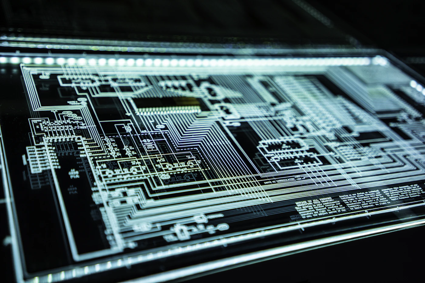
In the global power hierarchy of 2026, the traditional measures of strength—oil reserves, gold, or aircraft carriers—have been superseded by a single, microscopic unit of production: The Semiconductor Wafer. Advanced chips, those produced at nodes below 3 nanometers, are the foundational “oil” of the artificial intelligence era. Without these chips, the modern economy ceases to function. The construction of an advanced Semiconductor Fab (Yarı İletken Fabrikası) is the most complex, expensive, and strategically critical undertaking a nation or corporation can attempt.
A modern Fab is not just a factory; it is a monument to human engineering. The air inside a “Class 1” cleanroom is 10,000 times cleaner than the air in a hospital operating room. A single vibration from a distant highway can destroy a multi-million dollar batch of wafers. Our Institutional Semiconductor Simulator models the ruthless financial reality of this industry, where a 1% shift in “Wafer Yield” (Verim) can mean the difference between a billion-dollar profit and total financial insolvency.
The EUV Monopoly: ASML and the Art of Light
The core of every advanced Fab in 2026 is the Extreme Ultraviolet (EUV) Lithography machine. These systems, produced primarily by a single company (ASML), are the only machines in the world capable of printing circuit patterns at the 2nm scale. Each machine costs upwards of $350 Million and requires three Boeing 747s to transport.
If you do not have EUV, you are not in the advanced chip game. Our simulator factors in the number of EUV machines because they are the “bottleneck of throughput.” Each machine can process a finite number of wafers per hour. If you increase your Wafer Monthly Output (WSPM) but do not have enough EUV capacity, your “Cycle Time” increases, and your ROI collapses. In the 2026 silicon supercycle, securing a “Tooling Slot” for these machines is as difficult as the manufacturing process itself.
Yield is King: The Mathematics of Survival
In most industries, a 90% success rate is excellent. In semiconductor manufacturing, 90% yield on a new 2nm process is a miracle. Wafer Yield (Yarı İletken Verimi) is the percentage of functional chips on a completed wafer. During the early “Ramp-up” phase of a new Fab, yields can be as low as 20-30%, meaning 70% of the production is literal garbage.
Finansal modelimiz, verimi otomatik olarak %92.5 (olgun bir süreç için) seviyesinde hesaplar. Ancak, bu rakamın altına düşüldüğünde Annual Gross Revenue (Yıllık Brüt Gelir) hızla erir çünkü CapEx maliyetleri sabittir. Fabrikanın elektrik tüketimi, kimyasal kullanımı ve binlerce mühendisin maaşı, waferlar bozuk çıksa da ödenmek zorundadır. Bu yüzden yarı iletken dünyasında “Öğrenme Eğrisi” (Learning Curve) her şeydir; kim verimi daha hızlı yükseltirse, piyasayı o domine eder.

Capital Payback and the 24-Month Rule
Yarı iletken yatırımlarının en korkutucu tarafı **Amortisman (Depreciation)** süresidir. Bir Fab’ın içindeki makineler 5 yıl içinde teknolojik olarak eskir. Bu, her yıl milyarlarca dolarlık ekipmanın değerinin silinmesi demektir. Bu nedenle, bir Fab yatırımının **Payback Period (Geri Ödeme Süresi)** 5-6 yılı geçmemelidir.
Simülatörümüzde gördüğünüz $15 Milyarlık CapEx, sadece binanın kendisidir. Toplam yatırım genellikle $30 Milyarı aşar. 2026 yılında, bu seviyedeki bir sermayeyi sadece devlet teşvikleri (CHIPS Act vb.) ve devasa teknoloji şirketlerinin ön ödemeli siparişleri mümkün kılmaktadır. Eğer bir Fab, faaliyete geçtikten sonraki ilk 24 ay içinde %80 verime ulaşamazsa, ekonomik olarak “ölü” kabul edilir.
Conclusion: The Architecture of Absolute Power
2026 yılında, Global Ledger News olarak sunduğumuz bu simülasyon, bir iş modelinden daha fazlasıdır; bu, gelecekteki küresel gücün haritasıdır. Çip üretebilen bir ekonomi, yapay zekayı, savunma sanayini ve dijital finansı kontrol eder. Bu simülatörü kullanarak silikonun matematiğini çözün, EUV maliyetlerini optimize edin ve jeopolitik fırtınanın ortasında nasıl kârlı bir teknoloji kalesi inşa edileceğini öğrenin.
Ahmet
Director of Deep Tech & Semiconductor InfrastructureFounder of Global Ledger News. Based in Denizli, Türkiye, Ahmet specializes in the economic modeling of advanced silicon manufacturing, lithography logistics, and the geopolitical impact of “sovereign compute” in the 2026 global economy.